Semiconductors are the backbone of modern electronics, enabling the functionalities of devices we use daily. This detailed exploration breaks down the manufacturing process into its fundamental steps, mirroring the sophistication and precision required in this high-tech industry.
Historical Evolution of Semiconductor Manufacturing
The semiconductor industry has undergone a remarkable transformation, driven by groundbreaking advancements in research, design, and manufacturing. Over the last several decades, chips have evolved from simple components to complex integrated circuits with billions of transistors. This evolution has been fueled by the relentless pursuit of miniaturization and improved performance. The transition from 200 mm to 300 mm wafers marked a significant leap in manufacturing efficiency and cost reduction. These technological changes present a unique opportunity to optimally design the process control systems for the next generation fabs, further driving innovation and progress in the field.
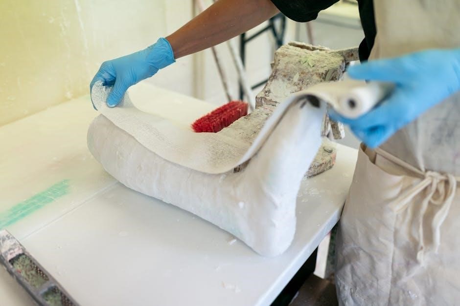
Wafer Manufacturing
The process begins with a silicon wafer. Wafers are sliced from a salami-shaped bar of 99.99 pure silicon (known as an ingot) and polished to extreme precision for semiconductor processing.
Silicon Ingot Production
The initial stage of wafer manufacturing involves silicon ingot production. This crucial step begins with melting high-purity silicon, often in a crucible. Precise temperature control is essential during this process. Impurities are meticulously removed to achieve the desired level of purity. A seed crystal is then introduced to initiate the crystal growth. This process grows a large, cylindrical single-crystal silicon ingot.
The Czochralski (CZ) method is commonly employed for this purpose. The ingot’s quality directly impacts the final semiconductor device performance. These ingots are then shaped into wafers, the foundation for microchip fabrication. Maintaining uniformity throughout the ingot is paramount.
Photolithography
Photolithography is a critical process involving multiple chemical and photographic processing steps. These steps transform a wafer of semiconducting material into electronic circuits. The process enables the creation of intricate patterns.
Photoresist Application
The photolithography process relies heavily on the application of a photoresist, a light-sensitive material. This material is meticulously applied to the wafer’s surface, forming a thin, uniform layer. The photoresist’s primary function is to act as a protective barrier, shielding specific areas of the wafer from subsequent etching processes. Accurate and consistent photoresist application is crucial because it ensures precise pattern transfer. Variations in the thickness or uniformity of the photoresist layer can lead to defects and irregularities in the final semiconductor device. Therefore, stringent controls and monitoring are implemented to maintain the quality of photoresist application throughout the manufacturing process.
Etching
Etching is a critical process where selected materials are removed from the wafer. This process is essential for creating intricate patterns and structures that define the circuits within the semiconductor device.
Etch Process Types
Etching processes in semiconductor manufacturing can be broadly categorized into two main types: wet etching and dry etching. Wet etching involves the use of liquid chemicals to remove materials. It offers high selectivity but can be less precise and isotropic. Dry etching, on the other hand, utilizes plasma or vapor-phase etchants for material removal.
Dry etching techniques provide better anisotropy and control over the etching process, making them suitable for creating fine features. Reactive Ion Etching (RIE) is a common dry etching method. The choice between wet and dry etching depends on the specific requirements of the manufacturing process and the desired characteristics of the final device.

Deposition
Deposition is a crucial step in semiconductor manufacturing, involving the addition of thin films onto the wafer surface. These films serve various purposes, including insulation, conduction, and acting as masks for subsequent processes.
Thin Film Deposition Techniques
Thin film deposition is a critical process in semiconductor manufacturing, entailing the application of thin layers of material onto a substrate. Several techniques are employed, each with its advantages and applications. Chemical Vapor Deposition (CVD) involves chemical reactions of gaseous precursors on the substrate surface, resulting in film growth. Physical Vapor Deposition (PVD), encompasses methods like sputtering and evaporation, where material is physically transferred from a source to the substrate. Atomic Layer Deposition (ALD) offers precise control over film thickness and composition by sequentially introducing different precursors, allowing for highly conformal films even on complex structures. These techniques are essential for creating functional layers in semiconductor devices.
Ion Implantation (Doping)
Ion implantation is a crucial process for modifying semiconductor properties. By introducing impurities, known as dopants, into the semiconductor lattice, its electrical conductivity can be precisely controlled, creating regions with desired characteristics.
Extrinsic Semiconductor Creation
Creating an extrinsic semiconductor involves intentionally introducing impurities into an intrinsic semiconductor to modify its electrical properties. This doping process is essential for tailoring semiconductors to specific applications. By adding elements with either more or fewer valence electrons than silicon, we create n-type or p-type semiconductors. N-type semiconductors have an excess of electrons, while p-type semiconductors have an excess of holes.
The controlled introduction of these impurities, typically through ion implantation or diffusion, allows precise control over the semiconductor’s conductivity and behavior. This ability to manipulate the electrical properties is fundamental to the function of transistors and other semiconductor devices, enabling the creation of complex integrated circuits.
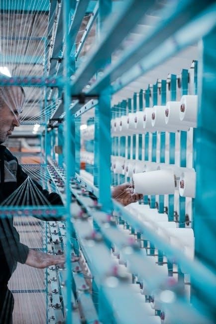
Metallization
Metallization is the process of depositing thin layers of metal onto the semiconductor wafer. It creates electrical interconnections between various components and provides pathways for signals and power distribution within the integrated circuit.
Metal Wiring Process
The metal wiring process involves depositing and patterning metal layers to create interconnections between different devices on the semiconductor chip. This intricate process ensures that electrical signals can travel between transistors and other components, enabling the circuit to function as designed. Different metallization techniques, such as sputtering and chemical vapor deposition (CVD), are employed to deposit thin films of metals like aluminum or copper. Photolithography and etching are then used to pattern the metal layers, creating the desired wiring network. The process is repeated for multiple metal layers to achieve complex interconnect schemes in modern integrated circuits, enabling complex and efficient signal routing.

Packaging
Semiconductor packaging is the final step in the manufacturing process, protecting the delicate chip. It involves encasing the die in a protective material and providing electrical connections to the outside world for functionality.
Backend Process Overview
The backend process, also known as packaging, is a crucial step in semiconductor manufacturing. It encompasses several key operations, beginning with die preparation, where individual chips are separated from the wafer. This is followed by die attach, where the chip is mounted onto a substrate or lead frame. Wire bonding, or other interconnect technologies, creates electrical connections between the chip and the external leads. Encapsulation then protects the chip from environmental factors like moisture and physical damage. The final steps involve testing and finishing to ensure the packaged device meets quality and performance standards, ready for integration into electronic systems.

Quality Control in Semiconductor Manufacturing
Quality control is paramount in semiconductor manufacturing. It involves rigorous testing and inspection throughout the process. This ensures the reliability, performance, and consistency of the final semiconductor devices for various applications.
Manufacturing and Quality Control
Manufacturing semiconductors involves a complex series of processes that transform raw materials into finished devices. Quality control during manufacturing is essential for ensuring the reliability and performance of these devices. This includes monitoring each step, from wafer fabrication to packaging, to detect and correct any defects. Advanced metrology techniques, such as electron microscopy and optical inspection, are used to identify imperfections. Statistical process control (SPC) is also employed to maintain process stability and minimize variations. Effective quality control not only improves product yield but also reduces costs and enhances customer satisfaction by delivering high-quality semiconductors.
No Responses